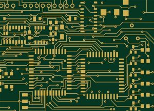
What Is Radar PCB?
Radar PCB is a type of electronic circuit board that is used to transmit and receive radio frequency signals. It can be used for a variety of applications including speed detection, distance measurement, and object identification.
They are also useful for ADAS systems like adaptive cruise control, forward collision warning, and active brake or lane change assist. In addition, they can help detect environmental hazards inside and outside the vehicle.
Solderability Examination
Solderability testing is performed to determine how well solder bonds to a component or PCB pad. This process is performed in order to increase the likelihood of a reliable solder joint forming and minimize the risk of failure. It is an important component test that should not be ignored by manufacturers, professionals and do-it-yourselfers alike.
There are two common methods for conducting solderability tests. The first method is known as dip-and-look testing. This method involves preconditioning, flux application and immersion of terminations in molten solder, if necessary.
The second method is known as Surface Mount Process Simulation (SMPS) solderability testing. This method involves the immersion of terminations in a solder pot of sufficient volume for the desired length of time, followed by an inspection for pinholes and other defects. The SMPS method also includes a steam aging step to ensure that terminations are properly aged before being immersed in the molten solder.
One method of measuring wicking properties of solder is by applying a test pattern with a continuous strip to a board which has been designed for evaluating cross machine solderability in accordance with this invention. The width of the strip along the continuous pattern is a critical parameter in this evaluation method.
Another method of measuring wickability is by using wetting balance analysis on the surface-based package. This method evaluates the wetting speed and strength of the liquefied solder on the assessment surface by plotting the force on the wetting balance arm as a time factor. The plot begins with a negative force and then increases gradually to indicate that wetting has taken place.
Generally, wetting occurs when the molten solder forms a comparatively uniform, smooth, and continuous film that adheres to the surface of a component. Non-wetting is a condition in which the liquefied solder partially sticks to the surface of a component and dewetting occurs when the molten solder withdraws from the surface.
Solderability testing is a crucial component test that should be conducted on all electronic packaging and circuit board assembly applications. This process is essential to ensuring that robust and reliable solder joints are formed for most applications, particularly when long-term component storage is involved.
Contamination Test
Radar PCBs are printed circuit boards that have a number of components and use RF-based materials. These boards are a vital part of the electronics industry and are used in a variety of applications, including automotive (millimeter-wave), industrial, and medical devices.
Radar sensors are Radar PCB a type of radar that can detect objects in the distance and determine their position. They can also be used in advanced driver assistance systems to prevent accidents.
The mmWave range of radar is highly effective for such applications, especially in the automotive sector. Future cars will need a variety of radar sensors to help them drive completely or partially autonomously.
These sensors are mounted on a radar PCB, which is made up of an antenna, power-management circuit, memory, and interface peripherals. The board is designed to withstand the high frequency of these signals and avoid interference.
The testing of a radar PCB is important for several reasons. It can ensure that the board meets its design specifications, helps detect possible errors during production, and improves the overall quality of the product.
There are a number of tests that are performed by Radar PCB, including X-ray examinations and scanning electron microscopy. These tests can identify defects, flaws, and issues relating to assembly & soldering.
Scanning Electron Microscopy is a non-destructive and precise test procedure that uses a visibly lit, high-powered microscope to examine a component’s construction. It can identify surface and interior defects while maintaining the sample in its pre-testing state.
It can also be used to evaluate the reliability of solder joints and ensure that storage conditions don’t degrade the quality of these components.
In addition, it can detect defects and flaws that are hidden within a circuit board. It can even reveal defects on the underside of a chip that aren’t visible through conventional inspection methods.
Contamination test is an important radar PCB testing procedure that helps eliminate potential contaminants during manufacturing. The test measures the amount of contamination that can get into the device and assesses it against the cleanliness standards set by the manufacturer.
Scanning Electron Microscopy
Scanning Electron Microscopy (SEM) is a powerful microscope used to observe the structure of solid materials. It has a magnification range of up to 500 times higher than a light microscope and produces images with resolutions on the order of 10 nm. SEM is a highly versatile imaging method that can be used in a variety of applications, from semiconductor inspection to microchip assembly.
SEMs produce high-resolution images of sample surfaces by generating a narrow beam of electrons and scanning the beam over the surface Radar PCB of the specimen. The process is similar to a confocal microscope; the SEM uses a column to emit a beam of electrons, a focusing lens to focus the beam on a small spot on the sample’s surface, and a detector that collects the resulting information to create an image.
The SEM can use a tungsten or lanthanum hexaboride cathode, which is heated to produce electrons, and a phosphor anode that absorbs the emitted electrons. These electrons then travel through a vacuum system to the sample’s surface where they interact with other molecules. This adsorption process creates secondary and backscattered electrons, which are detected with a specialized type of detector. These two types of imaging allow the SEM to detect and distinguish between different types of samples, enabling researchers to develop new materials more quickly.
Typically, SEMs operate in an extremely high vacuum to prevent atmospheric molecules from absorbing the emitted electrons and the resulting images. This vacuum is achieved by a series of pressure-limiting apertures that separate the gun from the sample chamber.
This technique allows the SEM to be used to view a wide range of samples, including liquids and biological materials. However, some SEMs also have the ability to perform environmental scanning, which allows them to operate in a low-vacuum environment while still maintaining the same high-resolution.
The SEM is a powerful tool for materials analysis, and Radar PCB uses it to examine the metallization of its circuit boards. This technique can identify problems with the metallization, such as internal wire dress or sealing lid voids, and determine if the solder is correctly applied.
Testing Procedures
Radar PCBs are used for a variety of tasks including speed detection, distance measurement, and object identification. They are commonly applied in automotive, military, and industrial applications, and can be purchased from various suppliers.
Testing Procedures performed by Radar PCB manufacturers include solderability examination, contamination test, and scanning electron microscopy (SEM). These tests check the quality of a board’s components and verify its assembly process. They can also reveal defects and flaws that are difficult to spot with visual inspection.
Solderability examination is an important test that is ideal for checking the strength and quality of a radar PCB’s solder mask application. This is because the masks must be applied correctly or the boards will fail. Additionally, it checks for solder oxidation and corrosion that can result in board failure.
Another key testing procedure that radar PCB manufacturers use is the burn-in test, which demonstrates how a device will perform under stressful conditions. This test enables manufacturers to evaluate the reliability of their products before beginning production.
This procedure is usually done in a high-temperature oven, which simulates the thermal stress that a radar device would experience during its operational life. This accelerated testing can help manufacturers identify potential issues and prevent the most common failures from occurring.
When designing a radar PCB, it is essential to ensure that the design is completely testable. This is especially true for RF devices and circuits, which are susceptible to overheating and other problems.
Ideally, the test should be conducted in an anechoic chamber to avoid any interference caused by other objects. This is because a clutter-free environment is crucial for calibrating the RF signals on the radar board.
Once the RF parameters are tested, the sensor can be compared against a reference. This allows the designer to see how well the radar PCB performs with its reference.
Aside from analyzing the performance of the radar PCB, this test can also determine the correct signal processing and filtering that should be applied to the radar signals. This will ensure that the resulting reflected signal is in good shape and can be used to accurately measure distances.