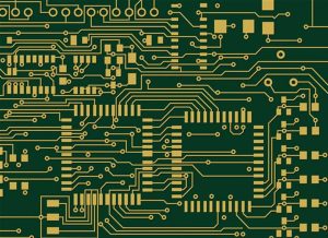
Factors to Consider When Designing a Multilayer PCB

In this article we’ll look at some of the important factors to consider when designing and manufacturing a multilayer pcb. These include signal integrity, cost, and design.
Designing a multilayer pcb
Designing a multilayer PCB can be a daunting task. It requires a lot of knowledge, experience, and extreme skills to get the job done. Multilayer PCBs are used in a variety of industries, including automotive, consumer electronics, aerospace, medical devices, and onboard computers. However, a PCB that is designed poorly could result in a product that is not reliable.
The first step in designing a multilayer PCB is to decide on the inner layer core. This can be a thin laminate material, or it can be a core that is thinner than the outer layer. A multilayer PCB can be created by using multiple layers of conductors, or a single layer of conductors can be placed between two or more layers of heat-protective insulation.
After selecting the core, the next step is to decide on the number of layers. Most multilayer PCBs contain four to eight layers, but the number can be as many as 100. Even numbers of layers make a circuit simpler, while odd numbers can cause problems. Choosing the right number of layers is a major consideration for manufacturers.
As the thickness of a PCB increases, the tolerances also increase. Tolerances are typically measured along the board, and they should be documented. If the total thickness of a PCB exceeds the optimum tolerances, it may result in bowing.
Multilayer PCBs also have to endure high temperatures. High temperatures can cause air to be removed between the layers, which is bad for reliability. Therefore, it is important to choose materials that offer the best operating temperature. Additionally, the materials should be able to withstand the pressures of the PCB.
Another consideration when designing a multilayer PCB is the cost of production. There are a number of factors that can impact the cost of a multilayer PCB, including the number of layers, the core thickness, and the amount of layers.
In addition, the complexity of the design and manufacturing process of a PCB can impact its cost. Many designers and manufacturers prefer to use even numbers of layers. But, there are some instances where an odd number of layers is necessary. For example, in the military, which is a highly-competitive industry, there are high-speed circuits that require a compact engineering design.
Another factor that should be considered when choosing a multilayer PCB is the layout. There are several benefits to multilayer PCB design, such as the ability to fit multilayer pcb into a smaller area, and the ability to increase the density of the layout. These advantages can help a designer avoid crosstalk problems and other issues that can prevent the performance of the circuit.
Finally, a multilayer PCB should have a good impedance. A poorly designed substrate can cause a product to have intermittent operation or increased emissions and crosstalk. On the other hand, a properly constructed PCB circuit board substrate can improve signal integrity, reduce electromagnetic radiation, and make a product more manufacturable.
Cost of designing and manufacturing a multilayer pcb
If you want to design and manufacture a multilayer PCB, there are some things you can do to help you save money. The number of layers you use, as well as their relative sizes, will have a direct effect on the cost of your product. Generally, you should try to choose the right mix of layers for the best results.
A good multilayer PCB should be able to withstand high temperatures and have a high degree of electrical stability. This makes it ideal for many applications, including household appliances, aerospace equipment, and medical devices. But it can also be expensive.
Unlike single layer PCBs, multilayer PCBs are made of multiple layers, which increases the complexity of the assembly process. They also require more time and resources. Moreover, a multilayer PCB is not cheap.
In addition to the obvious costs of materials, labor, and equipment, the cost of designing and manufacturing a multilayer PCB can increase exponentially. When looking for the best PCB manufacturer, it is important to look for a company that can handle the size of your project and its specifications. Whether you are a large or small business, a local PCB contract manufacturer can make your vision a reality.
Using a good CAD program can help you avoid making a costly mistake. You can even use a simulation to see how much your PCB will cost.
Another multi-layer PCB tip is to use the proper thickness of your material. This can help you to avoid bowing in your board, which can reduce its ability to perform in high temperatures.
Using the right finish on your PCB can also improve its shelf life. One option is to cover the surface of your PCB with ENIG (electrically conductive ink). However, it is important to consider that it will add to your overall cost.
Lastly, you should try to avoid crosstalk. Crosstalk can cause problems in the design and production of your PCB. For instance, if you use an asymmetrical design, you can end up with a twisted board that is difficult to wind.
Choosing the right type of PCB can also be a matter of personal preference. While some prefer high-end and expensive products, others look for low-cost options. You can use the internet to find the best deal for your project.
Fortunately, there are companies that specialize in manufacturing multilayer PCBs. These manufacturers will help you with the entire process, from designing to prototyping to mass production.
It’s worth the effort to find a reputable manufacturer. multilayer pcb Using a company that has been in the business for a long time will ensure your PCB has the best chances of success.
Regardless of which company you decide to use, it’s always a good idea to get a general idea of what the costs will be. Even a slight error in the production of your PCB can affect its performance.
Signal integrity
It is important to have good signal integrity when designing a PCB. This is especially true when the device is used in the high frequency regime. Whether you are a PCB designer or a designer of electronic devices, you need to have a thorough understanding of the techniques involved in signal integrity design. Incorrect layer planning or improper materials can degrade the performance of your PCB.
The proper combination of multiple planes, power and ground planes can enhance the signal integrity of a PCB. They help to prevent electromagnetic interference (EMI) from leaking into the circuit. These planes also provide good inter-plane capacitance, allowing for more efficient routing between levels. Moreover, these planes shield the board from external noise.
While a multilayer PCB can be made using as many layers as the board’s specification requires, it is important to plan ahead in order to get the most out of the design. An 8 layer stackup is one such approach that offers numerous benefits. If you are looking for a solution to signal integrity problems, consider the benefits of an 8 layer PCB.
One of the major reasons that an 8 layer PCB is a preferred choice is because it provides an excellent combination of EMI performance and mechanical stability. High layer count boards automatically have tight coupling between layers and are therefore suited for high-speed electronics. Likewise, they also allow for faster automated assembly processes.
As the number of conductive layers in a PCB increases, its thickness increases. However, if the copper in the board is too thin, it may cause electrical resistance. This can lead to undershoot, crosstalk and electromagnetic emissions. To avoid these issues, engineers should choose a PCB that has the correct copper thickness.
Multilayer boards should feature at least two conductive layers, but usually they have more. These layers are separated by insulating layers. Often, the outer layers are single-sided while the inner layers are double-sided. There are some multilayer boards that use partial planes on the top or bottom of the board.
When designing an 8 layer PCB, you must consider the signal integrity of each layer. In addition to the insulating and conductive layers, a power plane and ground plane are necessary to minimize crosstalk between the signals on the board.
For optimum power and ground integrity, a multilayer PCB should include a full metal ground and power plane. Full metal planes offer better power and ground integrity, as well as a cleaner power distribution network.
When designing a PCB, you must also consider the proper routing of signals. For instance, when a high-speed signal is routed in a group of signals, the quality of the signal will depend on the characteristics of the return path. Signal delay matching can help minimize skew in the group of signal lines. By minimizing the skew, you will be able to sample the signal accurately.

