
What Are Radar PCBs?
Radar is an efficient sensing technology used in a variety of applications. It is used for a range of tasks including speed detection and distance measuring.
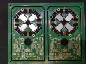
Typically, radar systems are built on a printed circuit board that includes the RF circuit, antennas, power-management circuit, memory and interface peripherals.
RF circuits
Radar PCBs need to be able to transmit and receive RF signals at high frequencies. This type of signal is used to detect objects and can penetrate clouds and other materials, such as rubber, to determine an object’s distance, velocity, and position when it’s in motion.
In addition, RF circuits need to meet steady-state performance goals for signal fidelity and noise, distortion, and interference. They must also be able to maintain their functionality under different environmental conditions, such as higher temperatures and humidity levels.
To meet RF design goals, designers need to use advanced simulation tools, PCB routing and layout tools, and layer stack design software. These tools help keep signal integrity intact while maintaining flexibility in design, so they can accommodate complex interconnects and unique trace and via structures.
1. Traces that connect RF components need to be short and spaced apart, so they can avoid energy coupling. This can cause crosstalk and noise induction, which reduces the accuracy of the RF signals.
2. RF CAD to CAM Documentation and Verification Designers need to provide accurate impedance trace dimensions and stack-up thicknesses to the PCB fabricator. They should also document RF critical areas and intended design dimensions.
3. Material selection
RF PCBs need to be made of the right materials for optimum performance. For example, FR4 laminates can be a good choice, but PTFE or thermoset polymer materials are preferred for high-frequency radar applications.
4. Substrate thickness
Radar PCBs need to be built on RF-grade substrates, such as RO4835 LoPro and RO3003. The substrate must be cured correctly for the proper bonding properties that will support the RF signals. This requires sequential lamination of the core and pre-preg substrates, as well as careful handling throughout fabrication.
Antennas
Radar PCBs use antennas that transmit light-speed signals to a target. The target then reflects the signal back to the Radar PCB radar PCB. This distance between the two devices determines the radar’s range.
The radar PCB sends periodic signals forming a wave of narrow rectangular pulses. The interval between the pulses determines the radar’s pulse repetition time. This is a very important aspect to consider when designing radar PCBs because it determines how far the signal can travel and how long it takes to receive an echo.
Designers also need to ensure that the antenna’s radiated energy isn’t reflected by metallic objects that may interfere with its functionality. This can impact the radar’s performance and cause it to malfunction.
Another factor to consider when designing radar PCBs is the antenna’s layer thickness. If the top layer is too thick, it can create resonance between the conductive elements of different layers, which affects the antenna’s performance.
This can result in reduced antenna gain and increased reflection of reflected waves. The optimum layer thickness is between one-eighth and one-quarter wavelength.
In addition, designers need to ensure that the antenna isn’t too close to other circuit components. This can lead to more signal interference and affect the device’s functionality.
The design process for a radar PCB begins with conceptualizing the circuit board’s intended application. This will help you decide on the circuit design’s operating temperature, component population, board size, and other features. Then, you can start the design process. It is a good idea to use a software program that has all of the necessary layout and simulation tools for your project.
Digital circuits
Digital circuits process binary data that is represented by the numbers 1 and 0. This data helps computers, electronic devices, and other systems understand information. Examples include a calculator or a mobile phone.
Modern Radar PCBs use a combination of digital and analog circuits. These are built using integrated circuits (ICs) that can perform several functions at a time instead of requiring separate components.
For example, a radar PCB uses digital circuits to transmit a radar pulse to a target and analyze the echo it produces. The signal is sent out at regular intervals. The delay between the signals is important for the device to receive the signal’s echo before sending out the next one.
Ideally, the pulse repetition time of a radar should be long enough to reach its target, but not too long. This will cause the target to move away from the radar before the signal reaches it, and the device will not be able to determine its distance accurately.
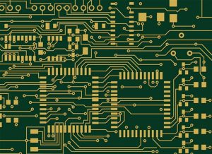
This is why a Radar PCB must be carefully designed. It must be equipped with circuit traces that do not interfere with each other. This is especially critical for RF & digital circuits that run at high speeds.
The material used for a Radar PCB must provide consistent relative dielectric constants across the board to prevent unwanted reflections and shifts in signal frequency and phase. This is particularly important Radar PCB when designing high-speed digital circuits that operate at 100 MHz or less. Historically, FR-4 was a popular choice for this type of circuit, but other materials are available that deliver better performance for these designs. These materials can be combined with woven glass or inorganic fillers.
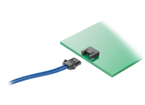
Through-hole mounting technology
Radar PCBs require robust and durable components that can withstand extreme temperatures, pressure, and other conditions. The through-hole mounting technology used in these boards is designed to withstand these factors and keep them working.
Through-hole mounting uses long leads that are inserted through holes in the board and then soldered to copper pads on opposite sides of the board. This process is more reliable and secure than surface mount technology (SMT).
The process also creates a stronger bond between the components and the PCB, which helps prevent component failure. It is a preferred technology for high-temperature environments and applications that undergo heavy physical stress.
Using through-hole technology during development and validation can help you achieve faster, more accurate product iterations with less unforeseen delays. As a result, you can have better control over your timelines and avoid costly errors that might delay your product’s launch date or lead to customer complaints.
Aside from a stronger connection with the PCB, through-hole components are typically more compact and easier to change than their SMT counterparts. They are also more flexible in terms of testing and prototype iterations.
Another advantage of this type of technology is that it can be used in small-lot projects without paying a third-party assembly service. As a result, the cost of fixtures and setup charges is reduced, which can save you money in the long run.
Both through-hole and surface-mount technologies have their advantages, but it is important to understand which one is right for your particular application. It is important to consider the following factors when making a decision:
Surface mount technology
The use of surface mount technology has grown rapidly over the years and has become a popular method of connecting components to printed circuit boards. It allows connections to be made on all sides of the board, which helps reduce manufacturing costs and time.
The process involves placing the components on a PCB using an automated machine called a pick-and-place machine. This is a much faster and more precise way to assemble the boards than through-hole mounting.
Once the component has been placed, the board is passed through a special machine that heats it just enough to melt all the solder paste used to connect the parts together. This ensures that the connections are strong and that all of the components are firmly attached to one another.
Surface mount technology also offers a few other benefits. The process can be more efficient and cost-effective than through-hole mounting, and it can also save space as components are generally smaller and require less depth to fit onto a board.
For example, a USB flash drive’s circuit board uses surface-mount components. These are small rectangular chips with numbers (resistors) or unmarked small square chips (capacitors).
Some manufacturers choose to use surface mount technology on their Radar PCBs because of the reliability and dependability it can provide. It also allows connections to be made on all sides of a board, which is an important factor in many electronics devices.